- 您现在的位置:买卖IC网 > Sheet目录2006 > LTC2498IUHF#TRPBF (Linear Technology)IC ADC 24BIT 16CH 38-QFN
LTC2498
25
2498ff
applications inForMation
remains HIGH for the duration of the conversion cycle.
Once the conversion is complete, the cycle repeats.
Typically, CS remains LOW during the data output state.
However, the data output state may be aborted by pull-
ing CS HIGH any time between the 1st rising edge and
the 32nd falling edge of SCK, see Figure 10. On the ris-
ing edge of CS, the device aborts the data output state
and immediately initiates a new conversion. In order to
program a new input channel, 8 SCK clock pulses are
required. If the data output sequence is aborted prior to
the 8th falling edge of SCK, the new input data is ignored
and the previously selected input channel remains valid.
If the rising edge of CS occurs after the 8th falling edge
of SCK, the new input channel is loaded and valid for the
next conversion cycle. If CS goes HIGH between the 8th
falling edge and the 16th falling edge of SCK, the new
channel is still loaded, but the converter configuration
remains unchanged. In order to program both the input
channel and converter configuration, CS must go HIGH
after the 16th falling edge of SCK (at this point all data
has been shifted into the device).
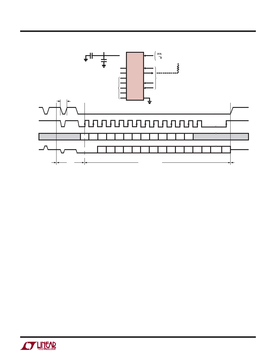
Internal Serial Clock, 3-Wire I/O, Continuous
Conversion
This timing mode uses a 3-wire interface. The conversion
result is shifted out of the device by an internally generated
serial clock (SCK) signal, see Figure 11. In this case, CS is
permanently tied to ground, simplifying the user interface
or transmission over an isolation barrier.
The internal serial clock mode is selected at the end of the
power-on reset (POR) cycle. The POR cycle is concluded
approximately 4ms after VCC exceeds 2V. An internal
weak pull-up is active during the POR cycle; therefore, the
internal serial clock timing mode is automatically selected
if SCK is floating or driven HIGH.
During the conversion, the SCK and the serial data output
pin (SDO) are HIGH (EOC = 1). Once the conversion is
complete, SCK and SDO go LOW (EOC = 0) indicating
the conversion has finished and the device has entered
the sleep state. The device remains in the sleep state a
minimum amount of time (1/2 the internal SCK period)
then immediately begins outputting and inputting data.
Figure 9. Internal Serial Clock, Single Cycle Operation
10F
0.1F
2.7V TO 5.5V
Hi-Z
2498 F09
CS
SCK
(INTERNAL)
SDI
SDO
CONVERSION
SLEEP
DATA INPUT/OUTPUT
CONVERSION
VCC
fO
REF+
REF–
CH0
CH7
CH8
CH15
COM
SCK
SDI
SDO
CS
GND
28
35
29
30
8
15
16
23
7
38
37
1,3,4,5,6,31,32,33,39
36
34
REFERENCE
VOLTAGE
0.1V TO VCC
ANALOG
INPUTS
= EXTERNAL OSCILLATOR
= INTERNAL OSCILLATOR
LTC2498
4-WIRE
SPI INTERFACE
EOC
BIT 28 BIT 27 BIT 26 BIT 25 BIT 24 BIT 23 BIT 22 BIT 21 BIT 20 BIT 19
BIT 29
BIT 30
BIT 31
BIT 18 BIT 17
BIT 0
1
2
3
4
5
6
7
8
9
10
11
12
13
14
32
1
0
EN
SGL
A2
A1
A0
EN2
IM
FA
FB
SPD
ODD
DON'T CARE
MSB
SIG
“0”
OPTIONAL
10k
VCC
<tEOCTEST
发布紧急采购,3分钟左右您将得到回复。
相关PDF资料
LTC2600IUFD#PBF
IC DAC OCTAL R-R 16BIT 20-QFN
LTC2602IMS8#TRPBF
IC DAC 16BIT DUAL R-R VOUT 8MSOP
LTC2604IGN-1#TRPBF
IC DAC 16BIT QUAD R-R OUT 16SSOP
LTC2605IGN-1#TRPBF
IC DAC 16BIT OCT I2C 16-SSOP
LTC2606IDD#TRPBF
IC DAC 16BIT I2C V-OUT 10-DFN
LTC2607IDE#TRPBF
IC DAC 16BIT R-R I2C 12-DFN
LTC2609CGN#PBF
IC DAC 16BIT R-R QUAD 16SSOP
LTC2621IDD-1#PBF
IC DAC 12BIT R-R 10-DFN
相关代理商/技术参数
LTC2499CUHF
制造商:Linear Technology 功能描述:ADC Single Delta-Sigma 7.5sps 24-bit Serial 38-Pin QFN EP
LTC2499CUHF#PBF
功能描述:IC ADC 24BIT DELTA SIG 38-QFN RoHS:是 类别:集成电路 (IC) >> 数据采集 - 模数转换器 系列:- 标准包装:1 系列:microPOWER™ 位数:8 采样率(每秒):1M 数据接口:串行,SPI? 转换器数目:1 功率耗散(最大):- 电压电源:模拟和数字 工作温度:-40°C ~ 125°C 安装类型:表面贴装 封装/外壳:24-VFQFN 裸露焊盘 供应商设备封装:24-VQFN 裸露焊盘(4x4) 包装:Digi-Reel® 输入数目和类型:8 个单端,单极 产品目录页面:892 (CN2011-ZH PDF) 其它名称:296-25851-6
LTC2499CUHF#TRPBF
功能描述:IC ADC 24BIT DELTA SIG 38-QFN RoHS:是 类别:集成电路 (IC) >> 数据采集 - 模数转换器 系列:- 标准包装:1,000 系列:- 位数:16 采样率(每秒):45k 数据接口:串行 转换器数目:2 功率耗散(最大):315mW 电压电源:模拟和数字 工作温度:0°C ~ 70°C 安装类型:表面贴装 封装/外壳:28-SOIC(0.295",7.50mm 宽) 供应商设备封装:28-SOIC W 包装:带卷 (TR) 输入数目和类型:2 个单端,单极
LTC2499CUHFPBF
制造商:Linear Technology 功能描述:24bit Delta Sigma ADC Temp Sens LTC2499
LTC2499IUHF#PBF
功能描述:IC ADC 24BIT DELTA SIG 38-QFN RoHS:是 类别:集成电路 (IC) >> 数据采集 - 模数转换器 系列:- 标准包装:1 系列:microPOWER™ 位数:8 采样率(每秒):1M 数据接口:串行,SPI? 转换器数目:1 功率耗散(最大):- 电压电源:模拟和数字 工作温度:-40°C ~ 125°C 安装类型:表面贴装 封装/外壳:24-VFQFN 裸露焊盘 供应商设备封装:24-VQFN 裸露焊盘(4x4) 包装:Digi-Reel® 输入数目和类型:8 个单端,单极 产品目录页面:892 (CN2011-ZH PDF) 其它名称:296-25851-6
LTC2499IUHF#TRPBF
功能描述:IC ADC 24BIT DELTA SIG 38-QFN RoHS:是 类别:集成电路 (IC) >> 数据采集 - 模数转换器 系列:- 标准包装:1,000 系列:- 位数:16 采样率(每秒):45k 数据接口:串行 转换器数目:2 功率耗散(最大):315mW 电压电源:模拟和数字 工作温度:0°C ~ 70°C 安装类型:表面贴装 封装/外壳:28-SOIC(0.295",7.50mm 宽) 供应商设备封装:28-SOIC W 包装:带卷 (TR) 输入数目和类型:2 个单端,单极
LTC2600CGN
功能描述:IC DAC OCTAL R-R 16BIT 16SSOP RoHS:否 类别:集成电路 (IC) >> 数据采集 - 数模转换器 系列:- 产品培训模块:Data Converter Fundamentals
DAC Architectures 标准包装:750 系列:- 设置时间:7µs 位数:16 数据接口:并联 转换器数目:1 电压电源:双 ± 功率耗散(最大):100mW 工作温度:0°C ~ 70°C 安装类型:表面贴装 封装/外壳:28-LCC(J 形引线) 供应商设备封装:28-PLCC(11.51x11.51) 包装:带卷 (TR) 输出数目和类型:1 电压,单极;1 电压,双极 采样率(每秒):143k
LTC2600CGN#PBF
功能描述:IC DAC OCTAL R-R 16BIT 16SSOP RoHS:是 类别:集成电路 (IC) >> 数据采集 - 数模转换器 系列:- 产品培训模块:Lead (SnPb) Finish for COTS
Obsolescence Mitigation Program 标准包装:50 系列:- 设置时间:4µs 位数:12 数据接口:串行 转换器数目:2 电压电源:单电源 功率耗散(最大):- 工作温度:-40°C ~ 85°C 安装类型:表面贴装 封装/外壳:8-TSSOP,8-MSOP(0.118",3.00mm 宽) 供应商设备封装:8-uMAX 包装:管件 输出数目和类型:2 电压,单极 采样率(每秒):* 产品目录页面:1398 (CN2011-ZH PDF)